1st Prize
Thomas Schopphoven, Andreas Gasser, Gerhard Maria Backes


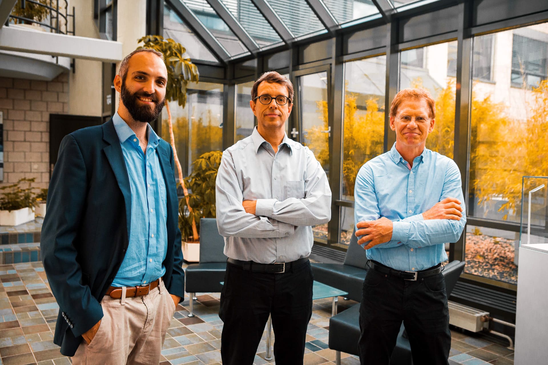
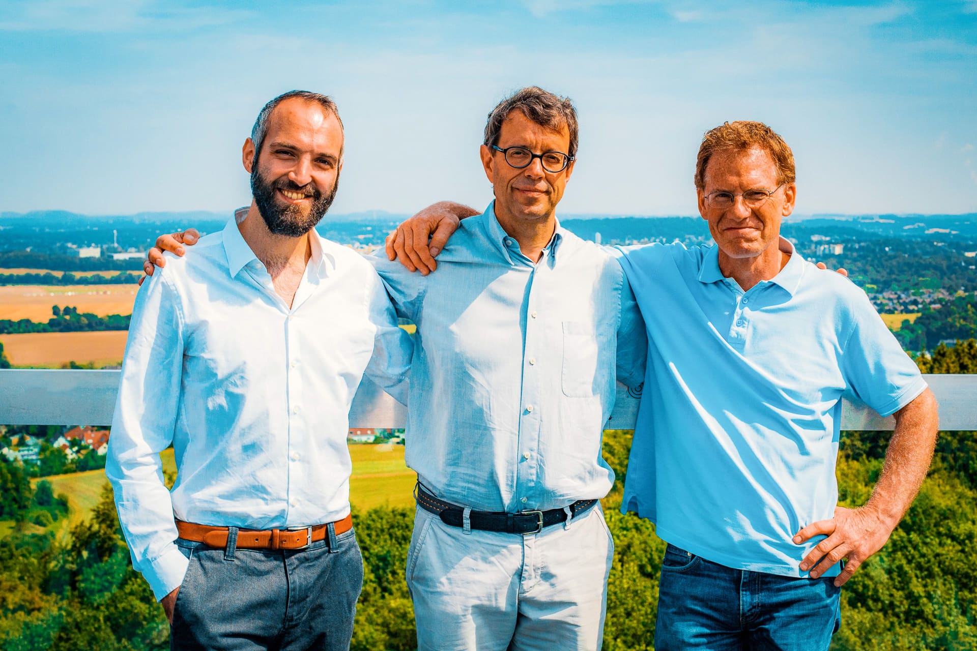
Project Group DELPHI:
Prof. Dr. Christian Koos (1,2), Alois Hauk (2), Philipp-Immanuel Dietrich (1,2), Dr. Nicole Lindenmann (1), Andreas Hofmann (3), Tobias Hoose (1), Muhammad Rodlin Billah (1), Matthias Blaicher (1)
(1) Institute of Microstructure Technology (IMT) and Institute of Photonics und Quantum Electronics (IPQ), Karlsruhe Institute of Technology KIT
Link Website | Link LinkedIn
(2) Vanguard Photonics GmbH
Link Website | Link LinkedIn
(3) Institute for Automation and Applied Informatics, Karlsruhe Institute of Technology KIT
Link Website | Link LinkedIn
Latest news
In 2020 Stefan Hell founded a new Start-up for the development of Nano microscope for brain research.
In 2013 Stefan Hell received the Nobel Prize in Chemistry.


EHLA is an enhanced Laser material deposition process where the metal powder particles are melted directly in the laser beam and not in the melt pool. This is a minor difference with a surprisingly powerful effect: process speeds can be greatly increased from a maximum of a few meters per minute to up to 500 meters per minute.


Headline Maintext
Nowadays, people are constantly checking their cell phones while going about their daily business: sharing photos and messages, using streaming services and accessing the worldwide web – whenever, wherever. The combination of fast mobile communications technology and the vast amount of information available on the Internet has led to an “explosion” of data needing to be transmitted. This instant availability of information would not be possible if it were not for fiber optic networks and lasers that can transmit information over long distances at sheer unimaginable speeds.
A single, whisper-thin optical fiber typically delivers data at speeds of several terabits per second. But the road-maps already include technologies that could develop this capacity even further – up into the range of petabits per second. The prerequisite for this level of throughput is an increasing number of integrated photonic components.
However, in contrast to electronics, a method has yet tobe found that can efficiently combine these photonic micro-chips. Therefore, developers either have to place all photonic circuits on a single chip, which requires complex production processes and allows for no flexibility, or the photonic chips have to be meticulously aligned with one another during production and then glued in place. Both of these options involve high production costs and result in optical systems that offer far fewer capabilities than integrated photonics.
The solution: photonic nanowires
Christian Koos had already noticed this gap in technology over ten years ago, while carrying out research for his dissertation at the Karlsruhe Institute of Technology (KIT). After a short stint working in industry, he became a professor at KIT and decided to find a solution for this as yet unsolved problem. His method of choice was 3D laser lithography, which had in the meantime reached a remarkable level of sophistication. This technology involves the use of an ultra-short pulse laser to cure plastics with a precision of several thousand nanometers (a nanometer is equal to one millionth of a millimeter). This process has shown itself to be ideal for fabricating optical waveguides between chips. Together with research partners from industry and the sciences, the young team at the KIT Institute began to research the basic technological requirements for using this process in industrial applications.
This yielded experimental evidence that waveguide connections – in addition to any other elements that maybe needed – can be fabricated between the optical components using specially adapted lithographical processes and the corresponding control software. An important milestone was thus achieved. The next logical step was to set up a start-up company for the development of ready-to-use systems for industry. A further important strategic partner for the young company Vanguard Photonics was quickly found: ficonTEC, a company that was already established on the market for photonic equipment on an international scale.

Brochure Headline
Lorem ipsum dolor sit amet, consectetur adipiscing elit, sed do eiusmod tempor incididunt ut labore et dolore magna aliqua. Ut enim ad minim veniam, quis nostrud exercitation ullamco laboris nisi ut aliquip ex ea commodo consequat.
Your contact person
Text for application or nomination...


